
Single crystal 300mm silicon carbide wafer
2026-01-28 08:35
On January 13, Wolfspeed announced achieving a major industry milestone by successfully producing 300mm (12-inch) single-crystal silicon carbide wafers. Leveraging the industry's largest and most foundational portfolio of silicon carbide intellectual property (with over 2,300 granted and pending patents worldwide), Wolfspeed is leading the charge in advancing silicon carbide technology to 300mm, paving the way for large-scale commercialization in the future.
This technological advancement marks a significant step forward for next-generation computing platforms, immersive AR/VR systems, and advanced power devices. By scaling silicon carbide to 300mm, Wolfspeed is unlocking new performance thresholds and manufacturing scalability for the world's most demanding semiconductor applications.
Wolfspeed Chief Technology Officer Elif Balkas stated, "Producing 300mm single-crystal silicon carbide wafers is a major technological achievement and the result of years of focused innovation in crystal growth, ingot, and wafer processing. This accomplishment enables Wolfspeed to support the industry's most transformative technologies, particularly key elements of the AI ecosystem, immersive AR/VR systems, and other advanced power device applications."
The Wolfspeed 300mm platform will consolidate high-capacity silicon carbide manufacturing for power electronics with advanced capabilities for high-purity semi-insulating substrates used in optical and RF systems. This integration will support new wafer-level integration across optical, photonic, thermal, and power domains.
As AI workloads push data centers to their power limits, the demand for higher power density, thermal performance, and energy efficiency will continue to accelerate. Wolfspeed's 300mm silicon carbide technology enables wafer-level integration of high-voltage power delivery systems, advanced thermal solutions, and active interconnects, extending system performance beyond traditional transistor scaling.
Next-generation AR/VR systems require compact, lightweight configurations that integrate high-brightness displays, wide fields of view, and efficient thermal management. Silicon carbide’s unique material properties, such as mechanical strength, thermal conductivity, and control of optical refractive index, make it an ideal choice for multifunctional optical architectures.
Beyond AI infrastructure and AR/VR, transitioning silicon carbide to the 300mm platform is an important step in scaling advanced power device production. Larger wafer diameters improve the ability to meet the growing demand for applications such as high-voltage grid transmission and next-generation industrial systems in a cost-effective manner.
Poshun Chiu, Chief Analyst of Compound Semiconductors at Yole Group, stated, "The 300mm breakthrough is not just a technical milestone; it also opens new opportunities for silicon carbide as a strategic material. It indicates that silicon carbide is advancing toward the next level of manufacturing maturity required for electrification, digitalization, and the AI era in the coming decade. This provides the market with a reliable roadmap for higher yields, better economic efficiency, and long-term supply security."
Related News
More >-
![Analysis of the properties and application fields of silicon carbide ceramics]()
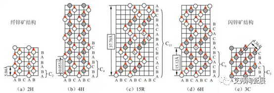
Analysis of the properties and application fields of silicon carbide ceramics
-
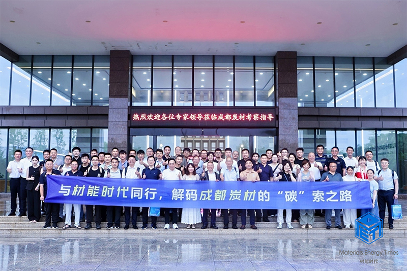
![2025 Second Third Generation Semiconductor Crystal Growth Technology Seminar]()
2025 Second Third Generation Semiconductor Crystal Growth Technology Seminar
-
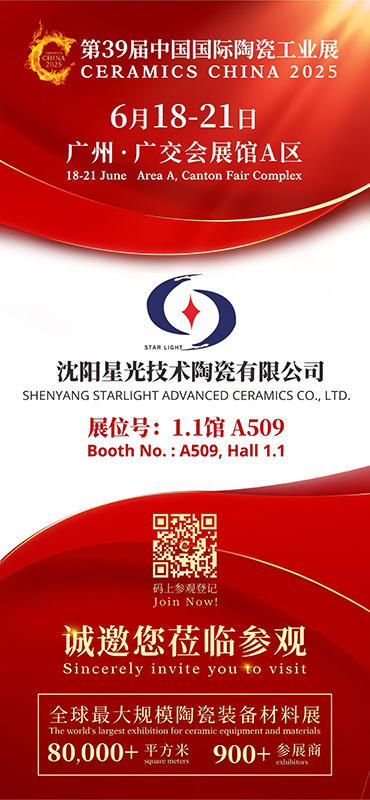
![The 39th China International Ceramics Industry Exhibition]()
The 39th China International Ceramics Industry Exhibition
-
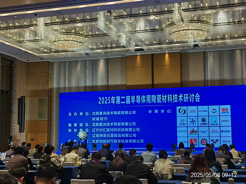
![2025 2nd Semiconductor Ceramic Materials Technology Symposium]()
2025 2nd Semiconductor Ceramic Materials Technology Symposium
-
![Ceramics Expo 2025 in the United States]()
Ceramics Expo 2025 in the United States
-
![Shenyang StarLight Advanced Ceramics: 30+ Years of Excellence in Silicon Carbide Solutions for the Semiconductor Industry]()
Shenyang StarLight Advanced Ceramics: 30+ Years of Excellence in Silicon Carbide Solutions for the Semiconductor Industry
-
![2025 China International Powder Metallurgy, Cemented Carbide and Advanced Ceramics Exhibition]()
2025 China International Powder Metallurgy, Cemented Carbide and Advanced Ceramics Exhibition
-
![]()
"Full-Chain Production Line for Silicon Carbide Structural Components in the Semiconductor Field
Get the latest price? We'll respond as soon as possible(within 12 hours)